
Popular Semiconductor Manufacturing Technology What do the advances in process technology mean for measurement? At the 2009 International Conference on Nano Measurement and Characterization Technology, participants exchanged views on the challenges that emerging technologies and materials pose for measurement technology. The first is that the chip size is close to the atomic and quantum levels, which has become a major problem in the measurement field. Such as increasing power consumption, process and device versatility, and reduced device and interconnect performance. For engineers, timely access to process information is essential, and the means of testing must be sufficient to meet the development of the process. .jpg) CMOS Ring Oscillator on Single Carbon Nanotubes For high k/metal gates, the main challenge is how to achieve certain performance while ensuring compatibility with standard CMOS fabrication. Advanced media that can replace traditional SiON materials must have high permittivity, good thermal stability, high mobility, low tunneling effects, and compatibility with metal electrodes. Corresponding to this trend, the support and development of measurement technology is one of the necessary conditions. Today, mask inspection must correspond to a complete lithography process in order to predict defects that may occur on silicon wafers in a timely manner. The inspection system should be able to provide complex illumination and match the precise structure of the lithography machine. Another popular area is 3D integration and through-silicon via technology (TSV), which will bring smaller size, lower power consumption and more powerful functionality to the chip, which is the next step in the development of semiconductor technology ( figure 2).
CMOS Ring Oscillator on Single Carbon Nanotubes For high k/metal gates, the main challenge is how to achieve certain performance while ensuring compatibility with standard CMOS fabrication. Advanced media that can replace traditional SiON materials must have high permittivity, good thermal stability, high mobility, low tunneling effects, and compatibility with metal electrodes. Corresponding to this trend, the support and development of measurement technology is one of the necessary conditions. Today, mask inspection must correspond to a complete lithography process in order to predict defects that may occur on silicon wafers in a timely manner. The inspection system should be able to provide complex illumination and match the precise structure of the lithography machine. Another popular area is 3D integration and through-silicon via technology (TSV), which will bring smaller size, lower power consumption and more powerful functionality to the chip, which is the next step in the development of semiconductor technology ( figure 2). 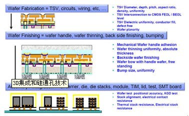 3D measurement technology meets the development of next-generation semiconductor technology New materials, new devices and structures will enable measurement technology to continue to evolve to meet new phenomena. High-k dielectrics, metal gates, and SOI are expected to be close to atomic size, and are highly likely to meet the 16nm node requirements. Although some new materials have already been applied to IC manufacturing, research and development on the corresponding measurement technology continues. Airgap and other low-k materials are also emerging. After years of academic research, people are familiar with carbon nanotubes, and know that carbon nanotubes are not practical, at least difficult to apply in nanoelectronics. The reason is that carbon nanotubes are difficult and reproducible to be incorporated into electronic devices. If the carbon nanotubes can be “cut†and unfolded into a stable surface, current state-of-the-art integrated circuit microfabrication technology can be used to achieve carbon material electronics (improving current silicon material electronics). A major discovery in the scientific community in recent years - graphene (Graphene) is this material. Graphene is a two-dimensional crystal composed of carbon atoms, and generally has a thickness of a single atomic layer or a diatomic layer of carbon atoms. Graphene (graphene) is its English name, which is related to graphite (graphite). Some people use "single-layer graphite". Graphene is a stable material and a semi-metal/semiconductor material with almost zero band gap. . It has a much higher carrier mobility (200,000 cm2/V) than silicon and has a mean free path of micron order and a very long coherence length at room temperature. Therefore, graphene is an ideal material for nanocircuits and an ideal material for verifying quantum effects. However, this material is also very difficult to measure (Figure 3). A graphite thin microscope is a necessary means of measuring this new material. One of the key issues is the number of layers of graphite in single and multilayer samples. TEM and low-energy electron microscopy (LEEM) are important detection devices for determining the number of layers, and multilayer slice simulations are an effective way to determine TEM detection capabilities and imaging conditions. LEEM can detect the number of layers and the morphology of the sample.
 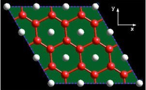 Graphene brings new challenges to measurement Diblockcopolymers are another new material that can be aligned on lithographic patterns and has the potential to increase lithographic pattern density under conventional lithographic conditions. And reduce line edge roughness (LER). The measurement of the material is mainly by x-ray scattering method, and the precision can reach a roughness of less than 0.5 nm. Because different chemicals have different resonance states, resonance scattering enhances the contrast between different chemicals to achieve accurate measurements.
CMOS Ring Oscillator on Single Carbon Nanotubes For high k/metal gates, the main challenge is how to achieve certain performance while ensuring compatibility with standard CMOS fabrication. Advanced media that can replace traditional SiON materials must have high permittivity, good thermal stability, high mobility, low tunneling effects, and compatibility with metal electrodes. Corresponding to this trend, the support and development of measurement technology is one of the necessary conditions. Today, mask inspection must correspond to a complete lithography process in order to predict defects that may occur on silicon wafers in a timely manner. The inspection system should be able to provide complex illumination and match the precise structure of the lithography machine. Another popular area is 3D integration and through-silicon via technology (TSV), which will bring smaller size, lower power consumption and more powerful functionality to the chip, which is the next step in the development of semiconductor technology ( figure 2). 3D measurement technology meets the development of next-generation semiconductor technology New materials, new devices and structures will enable measurement technology to continue to evolve to meet new phenomena. High-k dielectrics, metal gates, and SOI are expected to be close to atomic size, and are highly likely to meet the 16nm node requirements. Although some new materials have already been applied to IC manufacturing, research and development on the corresponding measurement technology continues. Airgap and other low-k materials are also emerging. After years of academic research, people are familiar with carbon nanotubes, and know that carbon nanotubes are not practical, at least difficult to apply in nanoelectronics. The reason is that carbon nanotubes are difficult and reproducible to be incorporated into electronic devices. If the carbon nanotubes can be “cut†and unfolded into a stable surface, current state-of-the-art integrated circuit microfabrication technology can be used to achieve carbon material electronics (improving current silicon material electronics). A major discovery in the scientific community in recent years - graphene (Graphene) is this material. Graphene is a two-dimensional crystal composed of carbon atoms, and generally has a thickness of a single atomic layer or a diatomic layer of carbon atoms. Graphene (graphene) is its English name, which is related to graphite (graphite). Some people use "single-layer graphite". Graphene is a stable material and a semi-metal/semiconductor material with almost zero band gap. . It has a much higher carrier mobility (200,000 cm2/V) than silicon and has a mean free path of micron order and a very long coherence length at room temperature. Therefore, graphene is an ideal material for nanocircuits and an ideal material for verifying quantum effects. However, this material is also very difficult to measure (Figure 3). A graphite thin microscope is a necessary means of measuring this new material. One of the key issues is the number of layers of graphite in single and multilayer samples. TEM and low-energy electron microscopy (LEEM) are important detection devices for determining the number of layers, and multilayer slice simulations are an effective way to determine TEM detection capabilities and imaging conditions. LEEM can detect the number of layers and the morphology of the sample. Graphene brings new challenges to measurement Diblockcopolymers are another new material that can be aligned on lithographic patterns and has the potential to increase lithographic pattern density under conventional lithographic conditions. And reduce line edge roughness (LER). The measurement of the material is mainly by x-ray scattering method, and the precision can reach a roughness of less than 0.5 nm. Because different chemicals have different resonance states, resonance scattering enhances the contrast between different chemicals to achieve accurate measurements. Guangzhou Yuquan Composite Material Co., Ltd , https://www.klyqfilm.com