

Fig. 1. (a) Schematic diagram of perovskite type solar cells; (b) Perovskite energy level diagrams with different silver injection rates; (c) Voltage-current efficiency curves of perovskite devices with different silver injection rates.
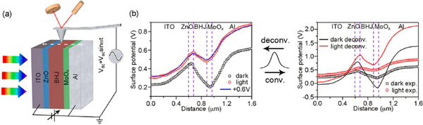
Figure 2. (a) Cross-section scanning Kelvin probe microscopy to characterize the energy level arrangement of trans-structured organic solar cells; (b) Restoring the true potential distribution of the device by deconvolution.
In recent years, new types of thin-film solar cells, such as organic/inorganic hybrid perovskite devices and organic photovoltaic devices, have attracted widespread attention due to their advantages of low cost, high efficiency, simple structure, and flexible carrying. For thin-film solar cells, the arrangement of the device's energy levels determines the microscopic physical processes such as separation, recombination, transmission, and collection of photo-generated carriers, and is one of the important determinants of device performance. How to effectively regulate and characterize the arrangement of device energy levels is an important starting point for understanding the working mechanism of devices, guiding the selection of materials and device process optimization.
Recently, the researcher Chen Lizhen of the Institute of Nanotechnology and Nano-Bionics of the Chinese Academy of Sciences has made new progress in the research on the regulation and characterization of the energy level arrangement of thin-film solar cells:
1. In organic/inorganic hybrid perovskite photovoltaic devices, an in-depth understanding of the interrelationships between material doping, energy level regulation, and device performance. First-principles calculations indicate that the outer electron orbitals of metal ions are an important determinant of the organic/inorganic hybrid perovskite band structure, which in turn affects the optical and electrical properties of the material. A number of research teams at home and abroad reported that a small amount of metal ions replacing Pb2+ can effectively improve device performance, but the mechanism of interaction between energy level structure evolution and device performance lacks in-depth research. Chen Lijiu's group used Ag+ to replace part of Pb2+ and introduce acceptor states into the perovskite, making the Fermi level of an originally n-type perovskite material move towards the center of the forbidden band, showing the properties of intrinsic semiconductors. The change effectively reduces the electron concentration in the perovskite, which is beneficial to the balanced transport of carriers. By optimizing the silver doping ratio, the crystallinity of the perovskite material is improved, and the film morphology and carrier kinetics are improved. Under the synergetic promotion of these factors, the efficiency of trans-structured perovskite planar heterojunction devices (ITO/Cu:NiOx/perovskite/PCBM/Ag) increased from 16.0% to 18.4% (Fig. 1). Furthermore, the interaction between perovskite carrier concentration and device performance was confirmed by an equivalent circuit model. Related research results were published on Nano Lett.
2. In organic thin-film photovoltaic devices, the energy level arrangement of trans devices was quantitatively characterized under device conditions. For the vertical closed type structure of thin-film solar cell layer stacks, there is currently no effective means to intuitively measure the energy level structure of the operating conditions of the device. Chen Lizheng's group reported a cross-sectional scanning cross-sectional SKPM at Nat. Commun. It can realize energy-level structure measurement under the operating conditions of short circuit, open circuit, dark state, and light, but the energy level The quantitative measurement of the arrangement is still pending. Further research, Chen Lijiu's group found that the pinpoint/cantilever beam convolution effect is an important factor affecting the quantitative measurement of the energy level structure of the device, in the presence of inversion-level abrupt change in the inversion device (ITO/ZnO/BHJ/MoOx/Al The convolution effect can even conceal the real potential distribution and lead to a misdirected built-in electric field. To solve this problem, they collaborated with Lu Shulong's research group to calibrate the tip transfer function of GaAs/GaInP heterojunction grown by molecular beam epitaxy. The deconvolution algorithm was used to remove the mean effect of the pin tip and restore the true energy level of the trans-device. Cloth (Figure 2). The relevant research results were published on Nano Energy, and they wrote monographs in the Journal of Physical Chemistry.
The research work was supported by professors such as Alex Jen from the University of Washington, Lu Shulong, and researchers from the Suzhou Nanometer Institute. The research work was supported by the National Natural Science Foundation of China, the Ministry of Science and Technology’s key R&D program, and the funding support and R&D conditions of the Chinese Academy of Sciences’ scientific research equipment project.
The In-Wall Bidet Frame is a sturdy iron frame specifically designed to provide support for wall-mounted bidets. By fitting into the wall, it effectively conceals the bidet's tank and plumbing, resulting in a modern and streamlined appearance for the bathroom.
Beyond its aesthetic advantages, the in-wall bidet frame offers several functional benefits. One of its primary advantages is the enhanced support it provides for the bidet fixture. This is particularly beneficial for larger individuals or those with limited mobility, as the frame ensures a stable and secure installation. The added support contributes to a comfortable and safe user experience.
The in-wall bidet frame is also height adjustable, allowing for customization to accommodate individual preferences and needs. This feature ensures that users can set the bidet at a comfortable height, promoting optimal usability and convenience.
Moreover, the space-saving design of the in-wall bidet frame is highly advantageous, especially in smaller bathrooms where floor space is limited. By fitting into the wall, the frame eliminates the need for additional floor space, effectively maximizing the available area. This can be particularly valuable for compact bathrooms, as it allows for a more efficient utilization of the available space.
In addition to space-saving benefits, the design of the in-wall bidet frame also facilitates easier cleaning and maintenance. With fewer exposed areas and nooks, there are fewer spaces for dust and grime to accumulate. This simplifies the cleaning process and helps maintain a hygienic environment.
In Wall Bidet Frame, Wall Hung Bidet Frame, Wall Hung Bidet Holder, In Wall Bidet Holder
Guangdong Fabia Intelligent Technology Co., Ltd , https://www.nbsmartfabiatoilet.com